Toshiba’s bescherming tegen elektrostatische ontlading voor analoge vermgenshalfgeleiders verbetert ESD-eigenschappen
TOKYO–(BUSINESS WIRE)– Toshiba Corporation heeft een beschermingsmiddel tegen elektrostatische ontlading (ESD) ontwikkeld voor toepassingen in analoge vermogenshalfgeleiders. Het middel is geproduceerd met behulp van geavanceerde verwerkingstechnologie op o,13μm, die de structuur van transistors optimaliseert en ESD-eigenschappen aanzienlijk verbetert. De bescherming tegen ESD is tot wel vier keer robuuster en de standaardafwijking is slechts één twaalfde van conventionele structuren. Dankzij een analyse van 3D-simulaties heeft stelde Toshiba ook in staat een mechanisme te ontdekken dat de transistorstructuur optimaliseert voor grotere ESD-robuustheid. Toshiba kondigde deze ontwikkelingen aan op ISPSD2016, een internationaal symposium over halfgeleiders dat op 14 juni 2016 plaatshad in Tsjechië.
Toshiba’s Electrostatic Discharge (ESD) Protection Device with 0.13μm Process for Analog Power Semiconductor Improves ESD Characteristics
TOKYO–(BUSINESS WIRE)– Toshiba Corporation (TOKYO:6502) has developed an electrostatic discharge (ESD) protection device for analog power semiconductor application, fabricated with advanced 0.13μm process technology, that optimizes the structure of transistor and significantly improves ESD characteristics. ESD protection is much more robust, up four times, and the standard deviation is only 1/12 that of the conventional structure. Analysis of 3D simulations has also allowed Toshiba to identify a mechanism for optimizing transistor structure to boost ESD robustness. Toshiba announced these advances at “ISPSD2016”, the international semiconductor symposium held in Czech on June 14, 2016.
This Smart News Release features multimedia. View the full release here: http://www.businesswire.com/news/home/20160615005479/en/
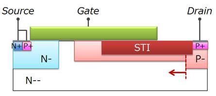
 Schematic cross-section of studied structure (Graphic: Business Wire)
Injections of ESD surges, whether from the human body or equipment, have the potential to destroy semiconductor devices, as ESD current flows cause local temperature increases inside silicon. ESD protection devices are required to protect internal circuit. This is especially true for analog power semiconductor devices required to apply 10V to 100V, which need a high rated voltage. In this case, ESD protection devices must ensure high current flow, which results in enlarged chip size. Shrinking the size of the ESD protection device is an issue in realizing more compact chips.
Using 3D simulation analysis of an ESD event, Toshiba found out that ESD induced destruction is caused by lattice temperature increase due to the current flowing at the highest electric field point. Modifying the transistor structure, which extending the drain low resistive region to the source direction and suppressing the lateral silicon resistance, shifts the current flow from the bottom of the drain to source direction and detaches it from the highest electrical field point. This optimized design was found to increase ESD robustness by up to four times and to decrease the standard deviation down to 1/12. In addition, the device size required to ensure HBM * ±2000V was cut by 68%.
Toshiba offers advanced analog process platforms, with 0.13μm process technology, that can be embedded with the transistors such as CMOS, DMOS, bipolar transistor and the passive devices such as resistor and capacitor. User can select a process suited to each application from three process platforms: “BiCD-0.13” is mainly for automotive (DMOS line up is up to 100V); “CD-0.13BL” is mainly for motor control drivers (DMOS line up is up to 60V); and “CD-0.13” process is mainly for power management IC (DMOS line up is up to 40V).
Toshiba plans to release products using the CD-0.13 process applied in this technology in 2017 and proactively continue to implement to other process platforms to improve electrostatic discharge characteristics.
* HBM (Human Body Model) : one of the parameter to indicate ESD robustness
About Toshiba
Toshiba Corporation, a Fortune Global 500 company, channels world-class capabilities in advanced electronic and electrical product and systems into three focus business fields: Energythat sustains everyday life, that is cleaner and safer; Infrastructure that sustains quality of life; and Storage that sustains the advanced information society. Guided by the principles of The Basic Commitment of the Toshiba Group, “Committed to People, Committed to the Future”, Toshiba promotes global operations and is contributing to the realization of a world where generations to come can live better lives.
Founded in Tokyo in 1875, today’s Toshiba is at the heart of a global network of 550 consolidated companies employing 188,000 people worldwide, with annual sales surpassing 5.6 trillion yen (US$50 billion). (As of March 31, 2016.)
To find out more about Toshiba, visit www.toshiba.co.jp/index.htm
View source version on businesswire.com: http://www.businesswire.com/news/home/20160615005479/en/
Contacts
Toshiba Corporation
Storage & Electronic Devices Solutions Company
Koichi Tanaka / Kota Yamaji, +81-3-3457-3576
Communication IR Promotion Group
Business Planning Division
semicon-NR-mailbox@ml.toshiba. co.jp
