
Toshiba ontwikkelt ‘s werelds eerste NAND-flashgeheugen uit 16 siliciumplaatjes met TSV-technologie
TOKYO–(BUSINESS WIRE)– Toshiba Corporation heeft vandaag bekendgemaakt dat het ‘s werelds eerste NAND-flashgeheugen gaat maken met gebruik van de technologie Through Silicon Via (TSV). Een prototype van het flashgeheugen, dat bestaat uit zestien op elkaar gestapelde blokjes geleidend materiaal, zal voor het eerst te zien zijn op de Flash Memory Summit 2015, die van 11 tot 13 augustus plaatsvindt in Santa Clara in de Verenigde Staten.
Momenteel worden NAND-flashgeheugens uit opgestapelde plaatjes bijeen gehouden door draad. TSV maakt daarentegen gebruik van verticale elektroden en via’s die door het silicium van de blokjes gaan en deze bijeen houden. Dit maakt zeer snelle invoer en uitvoer van gegevens mogelijk en vermindert het energieverbruik.
Toshiba Develops World’s First 16-die Stacked NAND Flash Memory with TSV Technology
TOKYO–(BUSINESS WIRE)– Toshiba Corporation (TOKYO:6502) today announced the development of the world’s first *1 16-die (max.) stacked NAND flash memory utilizing Through Silicon Via (TSV) technology. The prototype will be shown at Flash Memory Summit 2015, to be held from August 11 to 13 in Santa Clara, USA.
This Smart News Release features multimedia. View the full release here: http://www.businesswire.com/news/home/20150805006880/en/
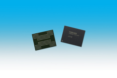 16-die Stacked NAND Flash Memory with TSV Technology (Photo: Business Wire)
The prior art of stacked NAND flash memories are connected together with wire bonding in a package. TSV technology instead utilizes the vertical electrodes and vias to pass through the silicon dies for the connection. This enables high speed data input and output, and reduces power consumption.
Toshiba’s TSV technology achieves an I/O data rate of over 1Gbps which is higher than any other NAND flash memories with a low voltage supply: 1.8V to the core circuits and 1.2V to the I/O circuits and approximately 50% *2 power reduction of write operations, read operations, and I/O data transfers.
This new NAND flash memory provides the ideal solution for low latency, high bandwidth and high IOPS/Watt in flash storage applications, including high-end enterprise SSD.
A part of this applied technology was developed by the New Energy and Industrial Technology Development Organization (NEDO).
|
The General Specification of Prototype |
||||||
| Package Type | NAND Dual x8 BGA-152 | |||||
| Storage Capacity (GB) | 128 | 256 | ||||
| Number of Stacks | 8 | 16 | ||||
| External Dimension
(mm) |
W | 14 | 14 | |||
| D | 18 | 18 | ||||
| H | 1.35 | 1.90 | ||||
| Interface | Toggle DDR | |||||
Note:
*1: As of August 6, 2015. Toshiba survey.
*2: Compared with Toshiba’s current products.
About Toshiba
Toshiba Corporation, a Fortune Global 500 company, channels world-class capabilities in advanced electronic and electrical product and systems into five strategic business domains: Energy & Infrastructure, Community Solutions, Healthcare Systems & Services, Electronic Devices & Components, and Lifestyles Products & Services. Guided by the principles of The Basic Commitment of the Toshiba Group, “Committed to People, Committed to the Future”, Toshiba promotes global operations towards securing “Growth Through Creativity and Innovation”, and is contributing to the achievement of a world in which people everywhere live safe, secure and comfortable society.
Founded in Tokyo in 1875, today’s Toshiba is at the heart of a global network of over 590 consolidated companies employing over 200,000 people worldwide, with annual sales surpassing 6.5 trillion yen (US$63 billion).
To find out more about Toshiba, visit www.toshiba.co.jp/index.htm
View source version on businesswire.com: http://www.businesswire.com/news/home/20150805006880/en/
Contacts
Toshiba Corporation
Semiconductor & Storage Products Company
Megumi Genchi / Kota Yamaji, +81-3-3457-3576
Communication IR Promotion Group
Business Planning Division
semicon-NR-mailbox@ml.toshiba. co.jp